
Read my article on important PCB designing considerations for a SMPS you may need to practice. We are referring a 230V AC to 5V DC 2A power supply which will be really interesting and useful because, this is equivalent to a 10W USB mobile phone charger.
A Switching Mode Power Supply(SMPS)
Power supply is an essential part used to maintain desired levels of voltages and currents in any electronic appliance. When it comes to operating an electronic circuit using domestic power supply, most of the time we need to convert higher AC voltage input to a lower level DC voltage and regulate the output values against the input and load fluctuations.
There are several configurations to do this power conversion and regulation process. Among those configurations, switching mode voltage converters are one the most efficient(up to 96% efficient) method compared to linear regulators which dissipate much power than SMPS. Nowadays, almost every circuit containing microcontrollers or microprocessors are powered with this SMPSs due to its higher efficiency and reliability. However, so called higher efficiency can only be achieved with a proper design including the critical PCB designing part.
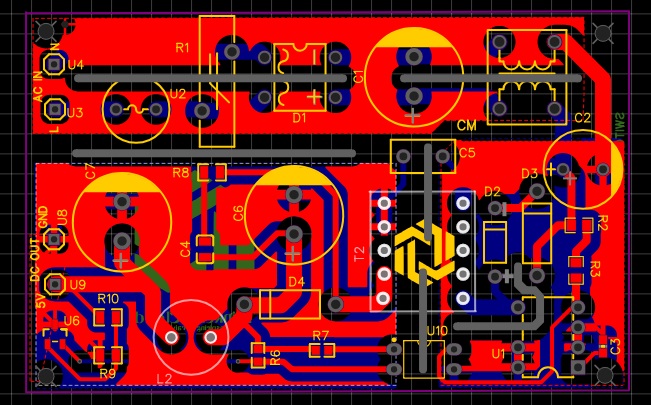
In this article we are going to discuss PCB designing considerations referring a 230V AC to 5V DC 2A power supply which will be really interesting since, this may be a very useful design equivalent to a 10W USB mobile phone charger. I used “EasyEDA” application to draw the schematic and PCB designing. Any other EDA software like Altium Designer, EagleCAD, ORCAD , Proteus can be used for this since, many of them have the tools which I used in here.
Components of the Design
This whole circuit can be separated into following main parts. I’m not going to explain the flow of a SMPS since we are more focusing on the PCB designing part.

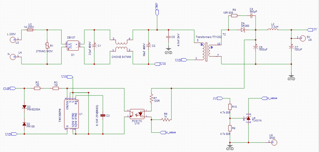
- Input with surge and over current protection (R1, U2):
R1 MOV is acting as an input surge protector by passing surge currents through itself, and U2 Fuse for fault protection within the circuit. - Rectification part (D1):
Bridge diode converts AC to DC. - Common mode EMI rejection filter (C1, CM, C2):
Rejects to common mode noise by CM common mode choke. - Driver and switching circuit (U1, C3):
Switching components (MOSFETs) and MOSFET driver circuit. - Clamping and Under-voltage protection (clamp:D2, D3 UnderV:R2, R3)
- Input-Output Galvanic isolation(T1): Isolate Input from output
- Rectifier and Snubber circuit (Rect: D6, Snub: R8, c4)
- Output filter ( C6, C7, L2)
- Feedback circuit (U6, U10, R6, R7, R9, R10): Feedback from output to the regulator part.
I have used a simple SMPS circuit using the TNY286 switching IC which contains the MOSFET and MOSFET driver and some other safety features inside.
Why PCB Designing so important?
Most of the electronic circuits contain microcontrollers or logic devices which are supposed to work under reliable voltage levels. In order to achieve this reliability, not only the schematic design with correct calculations, but also the PCB designing plays a crucial role to achieve desired results.
Since this Switching mode design contains some parts with high frequency switching currents, it becomes more important to have a proper PCB design to eliminate the electromagnetic interference for the output. Let’s go through the PCB design considerations described under the following topic.
PCB Design Consideration for SMPS
High voltage DC trace Separation
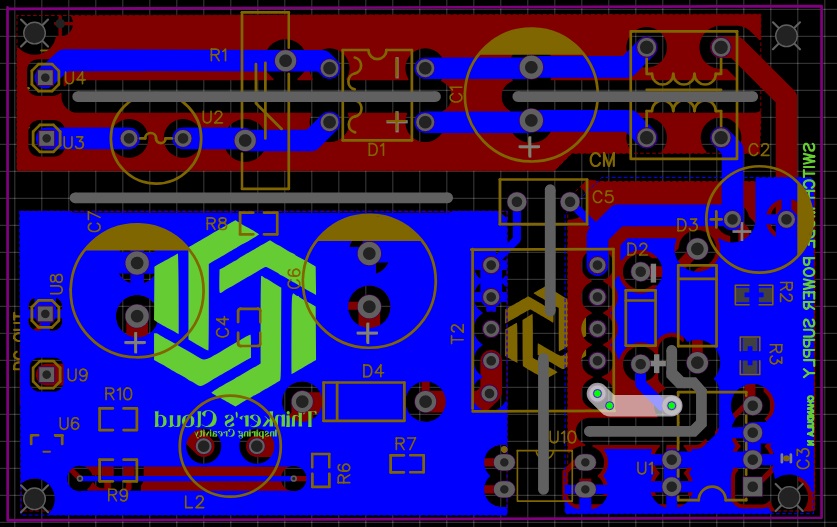
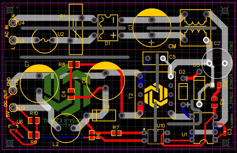
Traces which are carrying high voltage DC in a SMPS are always adding higher amount of noise to the signal lines due to the high frequency switching. Therefore, those lines needed to be separated from signal lines. In this Buck converter design, line which directly goes from the rectifier to the transformer must be separated. It is good to separate these lines using board cutouts Changing the high voltage lines and signal lines in to different layers also another good practice.
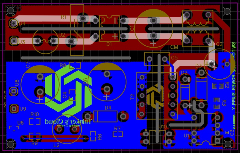
separation of Switching Traces
SMPS contains power elements like MOSFETs and drivers which perform the major role of a converter. When they are in the switching action, they contribute a huge amount of noise to the signal lines which maintains the output regulation process. Here in this design, MOSFETs and the MOSFET driver are integrated in to a single TNY268PN IC package. You can separate feedback or other signal lines from these lines using different layers or board cutouts. The line going out from the Drain pin of the IC is the high frequency switching line and that line has been separated using physical board cutouts as you see in below.
Shorten the length and Separate Feedback Traces
Feedback lines measure voltages or currents from output part and this lines are very sensitive even for small variations. Therefore, noisy supply lines or switching lines must be separated from feedback lines. Other than that, keeping feedback traces in short lengths and avoiding unnecessary higher widths can improve the quality of output.
Assign Widths for Power traces accordingly
Width of copper traces on a PCB is a crucial consideration when it comes to power supply designs or any other designs with high current drawing components. There is a maximum current which can be passed through a trace depending on the following factors.
- copper layer thickness (normally in oz)
- width of the copper trace
- temperature of then trace
You can calculate the maximum current carrying capacity using following formula.
Area = (Thickness x Width x 1.378)
Max_current = (k x (Temp_rise^b)) x (Area^c)
Where: k,b,c are constants,
According to IPC-2221A Documents (“Conductive Material Requirements”), their values for inner layers are as follows: k = 0.048 b = 0.44 c = 0.725
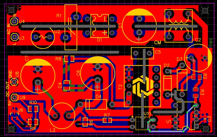
Generally, traces carrying high currents need to have a higher width than the signal carrying traces. After doing a proper calculation you can assign these widths if you know the maximum current flows of each trace. In this SMPS PCB design, I kept the high voltage input lines and high current carrying output DC lines with a higher width than feedback and other signal lines.
Placement of decoupling capacitors near the Inputs/outputs
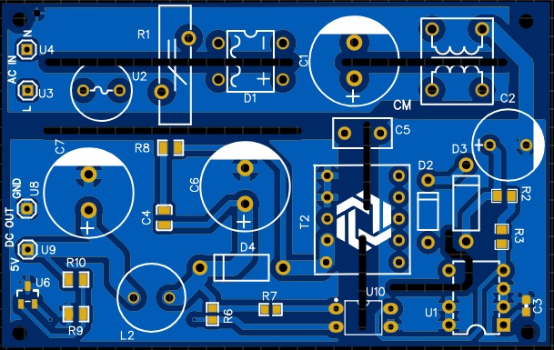
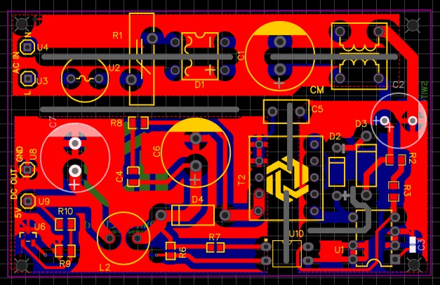
Adding Filter capacitors is another important part in any power supply to eliminate high frequency noise components from switching and AC sources. Both inputs and outputs can contain filter capacitors according to the design. They must be placed closer to the input or output connectors or signal pins of an IC. In this design I have placed input filter capacitor before the driver, C3 capacitor and C7 output filter capacitor
Separation between Transformer pads and Inductor Pads
When it comes to AC-DC SMPS circuits, the separation of the input form the output is done by a transformer by providing galvanic isolation. It also reduces ripples from the switching output. An adequate distance between primary and secondary pads of this transformer must be there in the PCB to achieve better results. Therefore, it is better to have a physical PCB board cutout or a good separation as in this example PCB.
The inductor connecting to the switching output also plays a major role from the output side of the circuit. It isn’t a good practice to route any traces in between the space of inductor pads since, those traces may be affected by EMI while passing high frequency currents through the inductor.
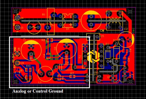
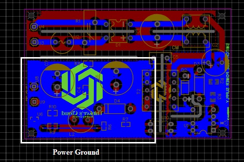
Ground planes separation
When it comes to adding copper zones (copper pouring) in to a power supply PCBs with feedback signals, specially connecting the ground paths through copper pour , you may need to pay a good attention to avoid ground bounce. Ground bounce is a deviation of the ground reference value of a circuit with a bouncing kind of voltage graph due to many external factors like neighbour switching components.
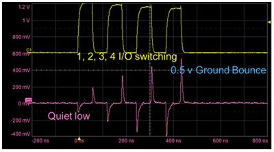
Reference : More Information About Ground Bouncing
Even if the ground connection of a SMPS is same for entire circuit in the electrical connections, it can be separated in to two paths as Power ground which carries higher currents with higher noise components and Analog ground which carries lower currents for feedbacks and regulation process. If you wish to add copper pour to ground planes it is a good practice to add separated ground planes to avoid noise from power ground to analog ground.


Leave a comment