
Beginning FPGA programming with Verilog
BEGINNING FPGA PROGRAMING WITH VERILOG
In my previous posts I have introduced Programmable Logic Devices(PLDs) and FPGAs which is a sub category of PLDs. Here I am going to show you how hardware implementation should be done with several basic examples with codes which I have done.
As a recap of previous posts, Field Programmable Gate Arrays, is a programmable logic device that is used to make hardware designs using programming. The software associated with it provide the user with the ability to implement his design in hardware level using behavioral programming.
VERILOG
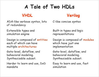
In this case I have used Verilog HDL. Verilog is a Hardware Description Language (HDL) which can be used to describe digital circuits in a textual manner. Learning Verilog is not that hard if you have some programming background. VHDL is also another popular HDL used in the industry widely. Verilog and VHDL share more or less same market popularity, but I chose Verilog since it is easy to learn ,it’s syntactical similarity to C language and most of our university assignments are recommended to do in Verilog. Once you are comfortable with Verilog, it should be easy learn VHDL as well.
Following is a little comparison between VHDL and Verilog.
If you are a begginer for Verilog programming you can learn Verilog easily througth this link.Click here to learn Verilog
Development board
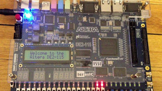
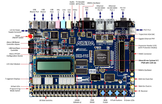
Here I have Used Altera (now it’s Intel) DE2-115 development board which has plenty of peripherals for our purpose. This has a Altera’s Cyclone IV FPGA chip. DE2 board is little bit expensive. However, we were able to borrow them form our university labs. You can use a cheaper board like Altera DE0-nano board rather than DE2 which also contain the same cyclone IV FPGA chip.
 DE2-115 board
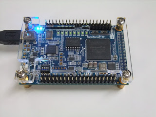
DE0-nano board
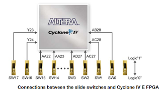
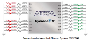
There are 27 user controllable green and red LEDs , 18 sliding on/off switches and 4 push button switches . In this board and most of other FPGA development boards contain separated GPIO (General Purpose Input output) pins which can be used to connect external peripherals such as LEDs or switches. So, you should not be worry about onboard peripherals of your board a lot.
You can download user manual ,driver software and other important information about the board from following links.
Download DE2-115 User manual
View details about DE2-115 board
Design flow
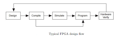
Typical design flow for hardware implementation is according to the above figure. You can get more knowledge on this flow with this link .
Let’s begin with a simple example which is a simple adder. In order to write the Verilog code, we can use a simple text editor such as windows note pad or using the smart text editor in an Electronic Design software tool which is specializes in Verilog coding.
Design
We are going to implement a one-bit full adder using Verilog. So, first of all you need to identify the need and make the flow of a adder using textual manner using Verilog syntax.
We are adding two bits and a carry-in bit and assign output in to two bits which are called sum and carry-out. There should be 3 input variables and 2 output variables. Here I have used behavioral model and assign outputs to the sum of all three inputs at ones. Using any text editor copy these Verilog code given bellow and save it as ‘full_adder.v’.
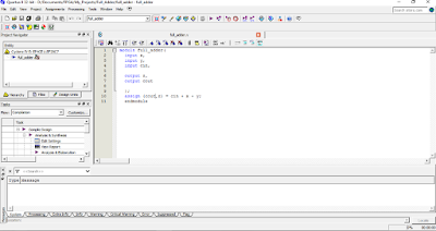
module full_adder(
                input x,
                input y,
                input cin,
                output z,
                output cout
                );
assign {cout,z} = cin + x + y;
                endmodule
Create a new project
Next, we will take the design we have created, to a specialized software suite where we can generate
the hardware requirement and deploy it on the FPGA. Because of we are using an Altera FPGA, we will use a compatible software suite called Altera Quartus II for our board. I assume you have properly installed Quartus II downloaded from Altera web site or from the Software disk comes with a development board. If you don’t have the software you can download web(free) edition with following link by registering in to the Altera site. Download Altera quartus II v12.0
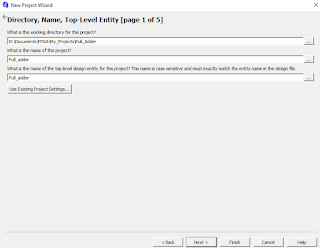
First, go to File menu in upper toolbar and select new. There you will see that a new window with list of file-type will appear and you must select new quartus ii project. Then a new project wizard window will appear. You should give a path and a name for the project. Top Level entity name also automatically changed with project name.
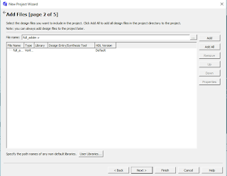
In the next tab you should give the path to our ‘full_adder.v’ file and click ‘add’.
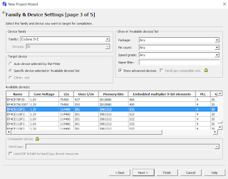
Next you should select the FPGA type according to your Development board or separated FPGA. Here we are using a Cyclone IV E FPGA and you can find the exact name of the device from their user manual or the box of the device.
After that there will see another two windows to complete the setup.You can skip them to finish the setup.Then the working area will appear with several pallets containing project details and files as the following image.
In the left side project Navigator panel you will see the project files and the hierarchical design of the project. There the only module in this project ‘full adder’ According to the user manual of the device you should identify which pins are assigned in to which peripheral and fill them in the location column of the table. Here we need only three switches as inputs and two LEDs as the output bits.
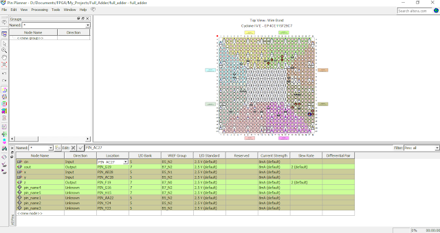 Here I have given some pin assignments of the DE2-115 board into Cyclone IV FPGA.
module is already assigned as the top Level entity. From the files tab you can select our Verilog file and do any change you want to do.
As you fill the table in you will notice that the pin assignment diagram changes according to that automatically. The newly assigned pins will be highlighted in red. Furthermore, the rows in the table will be colored according to the physical location of the pin on the FPGA.
Compilation
After completing the above steps for the design, it should be uploaded to the FPGA as a bitstream. In order to do so, we need to compile the design as follows. Go to Compilation>Start Compilation in the main Quartus II window. An automated toolchain starts which will translate the Verilog description in to a digital circuit, place the circuit into the FPGA and route the wire connections between logic elements and registers.
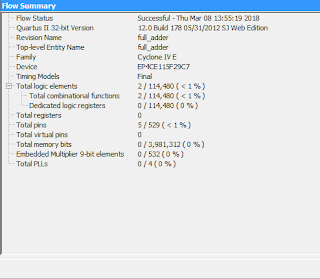
If everything has been set up properly, the compilation process should finish successfully without giving any errors or critical warnings
You could get a series of timing and utilization reports at each point of the compilation process and as shown below the final resource usage as the flow summery report will appear.
Program Hardware
After compilation we need to upload the bit-steam to the FPGA using a inbuilt programmer of the Quartus II software. Go to Tools > Programmer and open the programmer window.
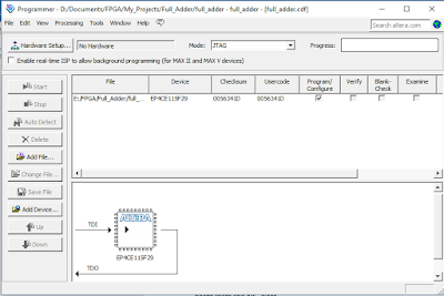 There you will see a uploadable bitstream file named “full_adder.so” will have been added to the programmer. If there is no such a file you have to add the file manually from the add file button.
So, we need to add our device. Plug the USB cable to FPGA board and connect it to the computer and powerup the Board with standard power supply for the board . Make sure you have installed popper drivers of the development board to the computer. Then go to the Hardware setup and select your board there and hit close.
Finally click the start button and it will upload the bit stream to the FPGA.
You can verify the design giving input bits using switches which you have assigned for the inputs and observing the results of sum and carry out bits using two output LEDs.
Simulate the Design
According to the design flow we have another intermediate step before the programming step called simulation. In order to simulate the project we need to write another code which is called a Test bench code with Verilog syntaxes. These codes are Verilog programs which are designed not towards building digital systems, but for testing them.
You might remember that the our ‘full_adder’ module we built in a previous step had inputs and outputs to communicate with the outside world using switches and LEDs. A testbench can be thought of as a bigger module which exists around the full_adder, connects to its ports and receives values. Usually a testbench has no ports for the outside, since it is supposed to be an independent isolated system.
Go to files>new>Verilog HDL file and copy following testbench code there. Save the file as ‘full_adder_tb.v’.
module full_adder_tb;
                reg x, y; // Inputs
                reg cin;
                wire  sum; // Outputs
                wire cout;
                // Unit Under Test (UUT)
                full_adder uut(x,y,cin,sum,cout);
                initial
                                begin
                                // Initialize Inputs
                                x = 0;y= 0;cin  = 0;
                                #10
                                // Wait 100 ns for global reset to finish
                                X=1;y=0;cin =1;
                                #10
X=0;y=1;cin=0;
#10
                                $finish;
                                end
   endmodule
Run the simulation
After adding the testbench file we are going to run the simulation using Altera’s simulator software called ‘ModelSim’. Quartus II software suite includes this third party simulation tool, which is one of the most powerful simulation tools existing in the industry.
In order to open simulator go to, Tools>Run Simulation Tool>RTL Simulation which will open ModelSim . After that a new window will open with ModelSim and there is the Library tab on the left side of the window. Go to ‘work’ library and see whether full_adder module is there. Selecting that will open the inputs and output variables
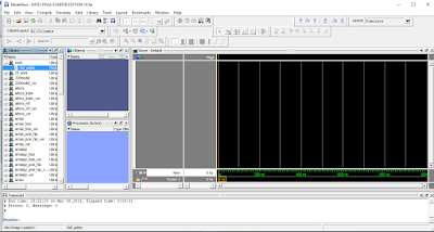
Then right click the Test Up Counter module in the Work library and select Simulate option . The software will initialize a simulation of the module, you will see Objects and Processes windows fill up with new entries and a new simulation window will open parallel to the Library window. You can add one or several variables to the Wave window and adjust the Run Length according to your test bench code run time.


Leave a comment