
Introduction to FPGAs
An Introduction to FPGAs
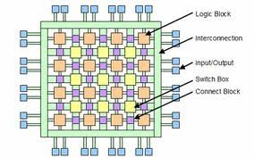
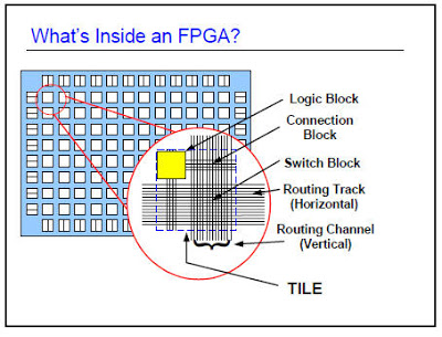
FPGA is an abbreviation of the field-programmable gate array and an integrated circuit designed to be reconfigured by a customer or a designer after manufacturing – hence it called “field-programmable”. The FPGA configuration is generally specified using a hardware description language (HDL), similar to that used for an application-specific integrated circuit (ASIC) which are not programmable and having fixed functions. FPGAs contain an array of programmable logic blocks having programmable AND gate and OR gate arrays, and a hierarchy of reconfigurable interconnects that allow the blocks to be “wired together”, like many logic gates that can be inter-wired in different configurations.
Logic blocks
The actual implementation of logic blocks depends upon the manufacturer and also the series of FPGA being used. The variations include the number of inputs and outputs, the general complexity of the logic block in terms of circuitry and the number of transistors used. This naturally has an impact on the amount of area consumed on the chip, and hence the size the silicon used. These logic blocks can be configured to have simple logic gates like AND and XOR or even perform a required very complex combinational function. In most FPGAs, logic blocks also include memory elements, which may be simple flip-flops or more complete blocks of memory in order to store inputs, outputs and sometimes inverted versions of both inputs and outputs.
Internal Connections
The routing inside the FPGA includes wires that can be interconnected using electrically configurable switches. In this way it is possible to link different points on the chip together and thus connect the different Common Logic Blocks in whatever way is required.
FPGAs vs ASICs
Although FPGAs offer many advantages, there are indeed some disadvantages. They are slower than equivalent ASICs which have same functionality of the comparing FPGA or other equivalent ICs, and additionally they are more expensive. (However, ASICs are very expensive to develop by comparison). This means that the choice of whether to use an FPGA based design should be made early in the design cycle and will depend on such items as whether the chip will need to be re-programmed, whether equivalent functionality can be obtained elsewhere, and of course the allowable cost. Sometimes manufacturers may select an FPGA design for early product (in preliminary development steps) when bugs may still be found, and then replace FPGA with an ASIC when the design is fully stable.
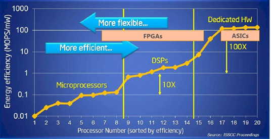
In view of the cost, they are not used in cheap and high-volume products, but instead FPGAs find applications in a variety of areas where complex logic circuitry may be needed, and changes may be expected. FPGA applications cover a wide range of areas from equipment for video and image processing, to circuitry for aerospace and military applications, as well as electronics for specialized processing, digital signal processing in many fields and much more.
Design using FPGAs
In view of the complexity of FPGAs, software is used to design the function of an FPGA and the designing process is started by the user providing a Hardware Description Language (HDL) definition or a schematic design.
Hardware Description Languages
There are two common hardware description languages,
- VHDL - VHSIC(Very High Speed IC) Hardware Description Language VHDL was initially developed by US Defense Department to research and develop very high speed integrated circuits in the 1980s. VHDL became IEEE Standard 1076 in 1987. Now, VHDL is mostly used to model digital and analog mixed signal circuits such as FPGAs and ASICs.
- Verilog- “Verification” + “Logic” Verilog was originally created by P. Moorby, P. Goel, C.-L. Huang, and D. Warmke in 1984 to model gates and perform simulation in a logic simulator. Verilog was acquired by Cadence in 1990 and became IEEE Standard 1364 in 1995. Now, Verilog is commonly used for designing and verification of digital circuits and analog or mixed signal circuits as well.
HDL vs Software Programming Languages
Verilog HDL is similar to C programming language in the side of case-sensitivity, keywords, operators, etc. VHDL is similar to Ada programming language since it was initially built based on Ada. The difference between Verilog and VHDL is presented here. Although there are similarities in syntax between HDLs (Verilog, VHDL) and software programming languages (C, Ada), FPGA programming is completely different from Software programming.
FPGA programming and software programming are differ due to the way that their instructions are executed. In term of the execution of instructions, instructions in software programming using languages(such as C, Ada, python and java) are sequentially executed while HDL (Verilog/ VHDL) instructions in FPGA programming are mostly parallelly executed (except blocking assignment in Verilog and variable assignment within a process in VHDL). More importantly, FPGA programming or FPGA design is about designing digital logic circuits to define the behavior of FPGAs while software programming is about the execution of a sequence of sequential instructions to perform a specific behavior in software.
Once this HDL definition or the schematic design making process has been completed the next task in the FPGA design process is to produce a netlist is generated for the particular FPGA family being used. This describes the connectivity required within the FPGA and it is generated using an electronic design automation tool. The netlist can then be fitted to the actual FPGA architecture using a process called place-and-route, usually performed by the FPGA company’s proprietary place-and-route software. Some commonly using software for above processes are,
- Xilinx -ISE (Integrated Synthesis Environment)
- Quartus – Altera These software tools produced by Xilinx and Altera companies for synthesis and analysis of HDL designs, enabling the developer to synthesize (“compile”) their designs, perform timing analysis, examine RTL diagrams, simulate a design’s reaction to different stimuli, and configure the target device with the programmer. Finally, the design is committed to the FPGA and it can be used in the electronic circuit board for which it is intended.
FPGA programming and Design Flow
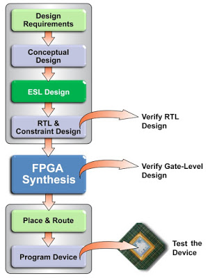
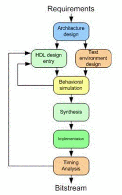
When we are using FPGAs for our designs as solutions for a particular problem there are several steps we need to follow in order to attain the required output. We divide these steps in the following way to get a flow.
-
First of all, we identify the project requirements and decompose our problem in to structural blocks which are having different functions and then make a document which contain all the details on the structural blocks, internal functions and interfaces using dedicated software.
-
We need to describe the above structure in hardware understandable way and we do that by writing a document by a formal HDL (Commonly Verilog and VHDL).
-
Also, we come up with a test bench document in order to ensure the functionality our HDL design which contain all the functions in HDL design for a test environment.
-
Next, we check the correctness of our HDL design by comparing the outputs HDL model and behavioral model by doing the Behavioral Simulation process.
-
Then the synthesis process done by a synthesizer software convert our HDL design in to a netlist which is a formally written digital circuit schematic.
-
Above netlist is now mapped onto a particular FPGA structure through a place and routing process (or called layout) which allocates FPGA connections and logic blocks. Then these configuration data are written to a file by bitstream generator.
-
Finally, timing analysis is done for check whether the implemented design satisfies the timing constraints specified by the user.
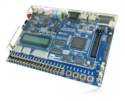
Testing the design on Development boards
According to the above design flow we obtain a bitstream file at the end of the final stage. We test that design using a FPGA development board by downloading the bitstream file to the FPGA through a programmer. These development board are available in market in different brands at different prices according to the FPGA’s performance and the development environment (Depending on the number of peripherals such as buttons, LEDs and LCDs and easiness of interfacing with external devices). Most popular and leading FPGA manufacturers in the world market are Altera and Xilinx. They have introduced a hundred of FPGA development boards with different features.


Leave a comment