
UART Communication Link Implementation with Verilog HDL on FPGA
This post is regarding a HDL implementation of a UART(Universal Asynchronous Receiver Transmitter) for one of our university fourth semester projects.
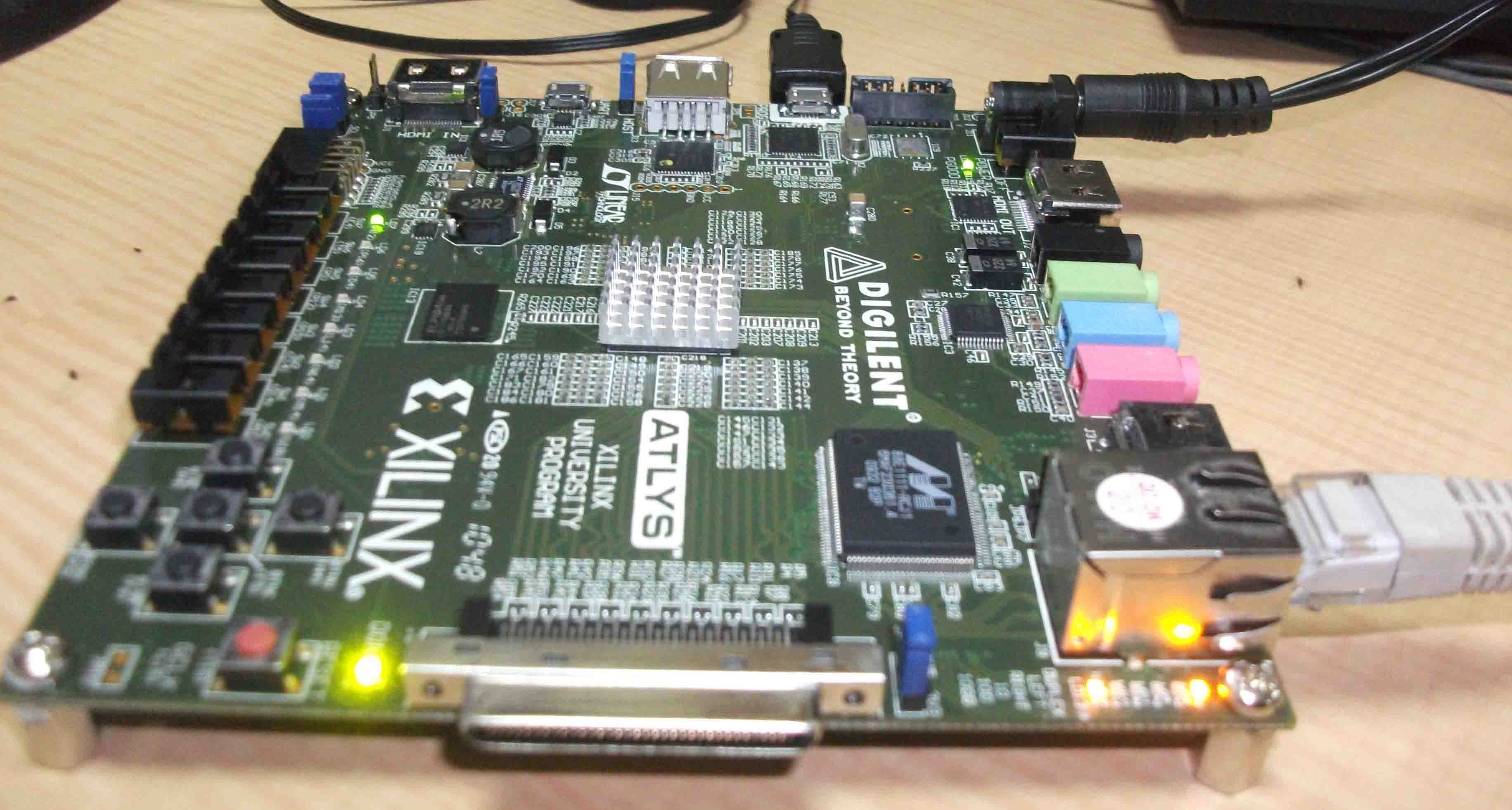
This was a group project of four group members. My group members are Chirath Diyagama, Isuru Nuwanthilaka and Dileepa Sandaruwan. For the project we were supposed to implement a UART link for a FPGA development board using Verilog as the HDL and send some data to another FPGA development board which also have a UART implementation. Here we used a Used a Digilant Atlys FPGA development board with a Xilinx FPGA. That board is actually expensive to buy. But we barrowed that one from our laboratory for this project. There is no problem if you want to implement this using another board.
Here we actually doing a bi-directional asynchronous communication between two FPGA board. Atlys FPGA board has certain number of switches as internal peripherals. We used each of them to represent a binary value. Using 8 switches we sent 8bit data words to other board. Then there are 8 LEDs assigned in to the output of the receiver and it will display the received data using that LEDs. After the communication between two boards we will talk about communication between a FPGA board and a Computer through USB connections. In order to do so the only need is a USB to UART bridge for your board. There are so many cheaper boards with Xilinx and Altera chips which you can find from online sites.
UART data frame
The structure of a UART frame can be illustrated as the above. Normally the data field can be varied from 4 bits to 9bits. There can be occupied a parity bit also.
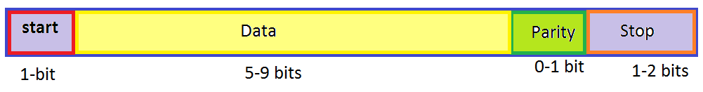
When we consider the UART data frames that has several data fields. Here we are using only these fields.
- Start Bit
- Data bits
- Stop bit/bits For our project we are using one start bit, eight data bits and two stop bits.
Baud Rate Generator
Every microprocessor and microcontroller require a clock signal because there are sequential circuits inside them. In our case also, there is an internal clock signal generator integrated onto the FPGA development board which provides a 100 MHz clock signal.
UART communication process also require a clock signal in order to generate and send each bit. But we cannot use the internal clock signal directly to our application. There are some standard Serial communication baud rates which the both transmitter and receiver parties should agree. Here we decided to use 115200 bits per second as the serial baud rate. We need a square shaped pulse at the above-mentioned clock rate in order to maintain a successful data communication.
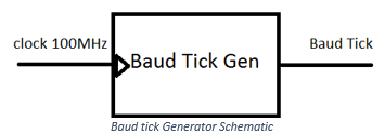
As a solution, we designed a Baud tick generator module using Verilog HDL and the schematic can be illustrated as shown in above figure. The only input is the internal 100Mhz clock signal and the output is the Required Baud tick signal.
Verilog Code for the Baud Tick Generator
module BaudTickGen(

                input clk, enable,

                output tick  // generate a tick at the specified baud rate * oversampling

);

parameter ClkFrequency = 100000000;                 //100MHz

parameter Baud = 9600;

parameter Oversampling = 1;

function     integer log2(input integer v);
                begin log2=0;
                while(v>>log2)
                                log2=log2+1;
                end
endfunction

localparam   AccWidth = log2(ClkFrequency/Baud)+8;  // +/- 2% max timing error over a byte
reg          [AccWidth:0] Acc = 0;
localparam   ShiftLimiter = log2(Baud*Oversampling >> (31-AccWidth));
                 // this makes sure Inc calculation doesn't overflow
localparam   Inc = ((Baud*Oversampling << (AccWidth-ShiftLimiter))...
                                                                ...+(ClkFrequency>>(ShiftLimiter+1)))/(ClkFrequency>>ShiftLimiter);

always @(posedge clk) if(enable) Acc <= Acc[AccWidth-1:0] + Inc[AccWidth:0]; else Acc <= Inc[AccWidth:0];
                assign tick = Acc[AccWidth];
endmodule
Here we are taking two inputs for our module as the input clock signal (which is a 100MHz ) and enable input to turn on or off the communication process. We have one output which is the baud tick signal.
parameter ClkFrequency = 100000000;                 //100MHz
parameter Baud = 9600;
Here we defined the Input Clock frequency in Hertz and the the desired baud rate in ticks per second.
Integration of Baud Generator
Here we integrate this baud tick generator module in to both UART Receiver module and UART Transmitter modules. Therefore, both of them taking input clock as our FPGA board’s internal clock signal which is a 100MHz signal and then inside each module Baud tick generator converts 100MHz square pulse in to a 115200 ticks per second baud signal.
UART Transmitter
Here we take three inputs to the Transmitter which are the parallel 8 set of input which contains the exact data we need to send, the starting input which act as a transmission on/off switch and the inbuilt clock signal from the FPGA development board.
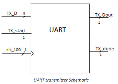
Inside this module we have our previously discussed baud tick generator and parallel to serial converter. Parallel data coming from 8 lines are time synchronously added together in to the rhythm of the baud tick and give to the out as a serial data stream on a single line. We also have another output to indicate an end of a packet called ‘Tx_done’.
Verilog Code for Transmitter
module UART_transmitter(
            input clk,
            input TxD_start,
            input [7:0] TxD_data,
            output wire TxD,
            output reg TxD_done//Txdone,

);

// Assert TxD_start for (at least) one clock cycle to start transmission of TxD_data
// TxD_data is latched so that it doesn't have to stay valid while it is being sent

parameter ClkFrequency = 100000000;         // 100MHz
parameter Baud = 115200;
wire TxD_busy;

/////////////////////////////////////Baud tick Generartor/////////////////////
wire BitTick;
BaudTickGen #(ClkFrequency, Baud) tickgen(.clk(clk), .enable(TxD_busy), .tick(BitTick));
//`endif
//////////////////////////////////////////////////////////////////
reg [3:0] TxD_state = 0;
assign TxD_ready = (TxD_state==0);
assign TxD_busy = ~TxD_ready;
reg [7:0] TxD_shift = 0;

always @(posedge clk)
begin
            if(TxD_ready & TxD_start)
                        begin TxD_shift <= TxD_data; end
            else
            if(TxD_state[3] & BitTick)                                                                                         //Data bits(byte) sending
                        begin TxD_shift <= (TxD_shift >> 1); end                //input byte is sening in each clock cycle one by one
            case(TxD_state)                                                                                                                                  //counting each bit
                        4'b0000 : if(TxD_start)
                                                            begin
                                                            TxD_state <= 4'b0100;
                                                            TxD_done<=0;
                                                            end
                        4'b0100: if(BitTick) TxD_state <= 4'b1000;  // start bit
                        4'b1000: if(BitTick) TxD_state <= 4'b1001;  // bit 0
                        4'b1001: if(BitTick) TxD_state <= 4'b1010;  // bit 1
                        4'b1010: if(BitTick) TxD_state <= 4'b1011;  // bit 2
                        4'b1011: if(BitTick) TxD_state <= 4'b1100;  // bit 3
                        4'b1100: if(BitTick) TxD_state <= 4'b1101;  // bit 4
                        4'b1101: if(BitTick) TxD_state <= 4'b1110;  // bit 5
                        4'b1110: if(BitTick) TxD_state <= 4'b1111;  // bit 6
                        4'b1111: if(BitTick) TxD_state <= 4'b0010;  // bit 7
                        4'b0010: if(BitTick) TxD_state <= 4'b0011;  // stop1
                        4'b0011: if(BitTick)                                                                                          // stop2
                                                            begin
                                                                        TxD_state <= 4'b0000;
                                                                        TxD_done<=1;
                                                            end
                        default: if(BitTick) TxD_state <= 4'b0000;
            endcase
end

assign TxD = (TxD_state<4) | (TxD_state[3] & TxD_shift[0]);  // put together the start, data and stop bits
endmodule
Here we are calling the Baud tick generator from the inside of the transmitter to sample the input data.
UART Receiver
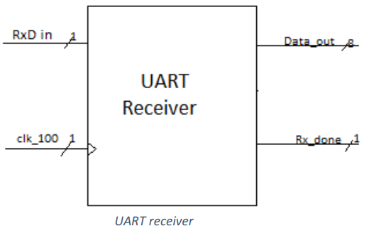
UART receiver taking two inputs which are input clock signal and the serial data input which is carrying a serial data stream sampled in a standard Baud Rate. Input serial data is again formed in to a set of 8 data lines after each packet is arrived in to the receiver.
Verilog Code for Receiver
module UART_receiver(
            input clk,
            input RxD,
            output reg Rx_done=0,
            //output reg RxD_data_ready = 0,
            output reg [7:0] RxD_data = 8'd0  // data received, valid only (for one clock cycle) when RxD_data_ready is asserted

              // asserted when no data has been received for a while
            //output reg RxD_endofpacket = 0  // asserted for one clock cycle when a packet has been detected (i.e. RxD_idle is going high)
);

parameter ClkFrequency = 100000000; // 100MHz
parameter Baud = 115200;
parameter Oversampling = 8;  // needs to be a power of 2
// we oversample the RxD line at a fixed rate to capture each RxD data bit at the "right" time
// 8 times oversampling by default, use 16 for higher quality reception
wire RxD_idle;


////////////////////////////////
reg [3:0] RxD_state = 0;
//reg RxD_data_ready = 0;

`ifdef SIMULATION
wire RxD_bit = RxD;
wire sampleNow = 1'b1;  // receive one bit per clock cycle

`else
wire OversamplingTick;
BaudTickGen #(ClkFrequency, Baud, Oversampling) tickgen(.clk(clk), .enable(1'b1), .tick(OversamplingTick));

// synchronize RxD to our clk domain
reg [1:0] RxD_sync = 2'b11;
always @(posedge clk) if(OversamplingTick) RxD_sync <= {RxD_sync[0], RxD};

// and filter it
reg [1:0] Filter_cnt = 2'b11;
reg RxD_bit = 1'b1;

always @(posedge clk)
if(OversamplingTick)
begin
            if(RxD_sync[1]==1'b1 && Filter_cnt!=2'b11) Filter_cnt <= Filter_cnt + 1'd1;
            else
            if(RxD_sync[1]==1'b0 && Filter_cnt!=2'b00) Filter_cnt <= Filter_cnt - 1'd1;

            if(Filter_cnt==2'b11) RxD_bit <= 1'b1;
            else
            if(Filter_cnt==2'b00) RxD_bit <= 1'b0;
end

// and decide when is the good time to sample the RxD line

function integer log2(input integer v); begin log2=0; while(v>>log2) log2=log2+1; end endfunction

localparam l2o = log2(Oversampling);
reg [l2o-2:0] OversamplingCnt = 0;
always @(posedge clk) if(OversamplingTick) OversamplingCnt <= (RxD_state==0) ? 1'd0 : OversamplingCnt + 1'd1;
wire sampleNow = OversamplingTick && (OversamplingCnt==Oversampling/2-1);
`endif

// now we can accumulate the RxD bits in a shift-register
always @(posedge clk) begin
//if(Rx_done) Rx_done =0;
case(RxD_state)
            4'b0000: if(~RxD_bit)
                                                begin
                                                RxD_state <= `ifdef SIMULATION 4'b1000 `else 4'b0001 `endif;  // start bit found?
                                                Rx_done<=1'b0;
                                                //Rxdone<=0;
                                                end
            4'b0001: if(sampleNow) RxD_state <= 4'b1000;  // sync start bit to sampleNow
            4'b1000: if(sampleNow) RxD_state <= 4'b1001;  // bit 0
            4'b1001: if(sampleNow) RxD_state <= 4'b1010;  // bit 1
            4'b1010: if(sampleNow) RxD_state <= 4'b1011;  // bit 2
            4'b1011: if(sampleNow) RxD_state <= 4'b1100;  // bit 3
            4'b1100: if(sampleNow) RxD_state <= 4'b1101;  // bit 4
            4'b1101: if(sampleNow) RxD_state <= 4'b1110;  // bit 5
            4'b1110: if(sampleNow) RxD_state <= 4'b1111;  // bit 6
            4'b1111: if(sampleNow) RxD_state <= 4'b0010;  // bit 7
            4'b0010: if(sampleNow)                                       // stop bit
                                                begin
                                                            RxD_state <= 4'b0000;
                                                            Rx_done <= 1'b1;
                                                            //Rxdone<=1;
                                                end
            default: RxD_state <= 4'b0000;
endcase
end

always @(posedge clk)
if(sampleNow && RxD_state[3]) RxD_data <= {RxD_bit, RxD_data[7:1]};

`ifdef SIMULATION
assign RxD_idle = 0;
`else
reg [l2o+1:0] GapCnt = 0;
always @(posedge clk) if (RxD_state!=0) GapCnt<=0; else if(OversamplingTick & ~GapCnt[log2(Oversampling)+1]) GapCnt <= GapCnt + 1'h1;
assign RxD_idle = GapCnt[l2o+1];

`endif

Endmodule
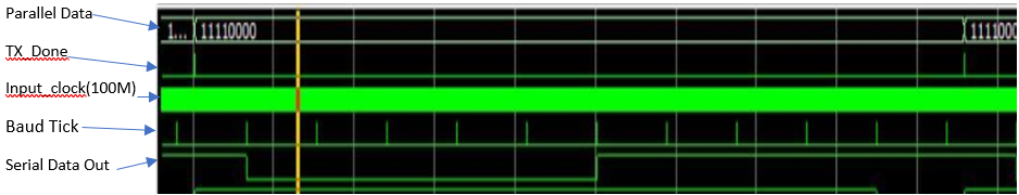
Output from the Simulator


Leave a comment